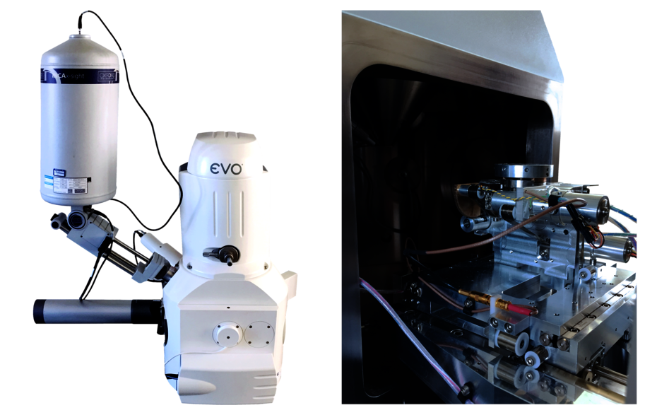
Scanning Electron Microscope
The scanning electron microscope (SEM) is an instrument in which an electron beam generated by a current-carrying filament is directed through magnetic lenses against the surface of the sample to be analysed. The interaction between the electrons and the sample surface generates signals that are then directed towards specific sensors. In particular, in the microscopes in the laboratory, it is possible to analyse back-scattered electrons (Back-Scattered-BSE), which give information on the distribution of elements in the material, and secondary electrons (SE), which give information on surface morphology. With such microscopes, it is possible to analyse structures that can be as small as a few tens of nanometres (SEM) or as large as a nanometre (FE-SEM). The instruments are also equipped with an EDXS probe, which makes it possible to perform a semi-quantitative chemical analysis of the analysis area by analysing the X-rays emitted by the sample through interaction with the electron beam. The SEM microscope is also equipped with an EBSD probe that allows crystallographic analysis of the material at the microscopic level, providing information on the crystallographic texture of the material itself. This instrument is also equipped with a device for micromechanical testing in the chamber up to maximum loads of 5kN.
The micromechanical tester was acquired through DPIA's strategic plan in collaboration with the SIMED, SMACT3 and LAMA research groups. Samples that can be analysed with the SEM are of a maximum size of 5 cm x 5 cm x 2 cm (l x w x h), while for the FE-SEM they are of the same size as the hot-embedded samples (cylinders with a diameter of 3 cm x 2 cm). The instruments are mainly used for:
Fractographic analysis;
Microstructural characterisation at the nanometric level;
Determination of thin film thicknesses;
Crystallographic analysis of materials (mapping);
Micromechanical properties of materials;
Characterisation of powders;
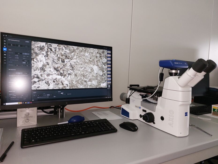
Light Optical Microscope (LOM)
An optical microscope is an instrument that allows the microstructure of a sample to be analysed by means of light directed towards the sample through optical objectives and then reflected back to eyepieces or a digital image/video capture system. The reflected light will result in an enlarged image of the material being analysed. With the supplied microscopes it is possible to analyse samples up to 1000X in different modes of analysis: bright field (classical analysis), dark field (better defines the asperities that give excusable colouration in bright field), polarised light and interferential contrast (polarised light with 3D effect). In addition to digital cameras, the microscopes supplied are also equipped with advanced image analysis software that enables measurements or evaluations of the various entities viewed under the microscope to be carried out.
The analyses that can be performed with such instruments are:
Inclusional analysis;
Grain size analysis;
Phase distribution analysis;
Thickness analysis;
Small-scale geometric measurements;
In addition, there are also stereographic microscopes that are used to perform high depth-of-field analyses, compared to the metallographic microscope, but at lower magnification. Such microscopes are used for:
dimensional evaluations;
Phase assessment at the macroscopic level;
Fractography;
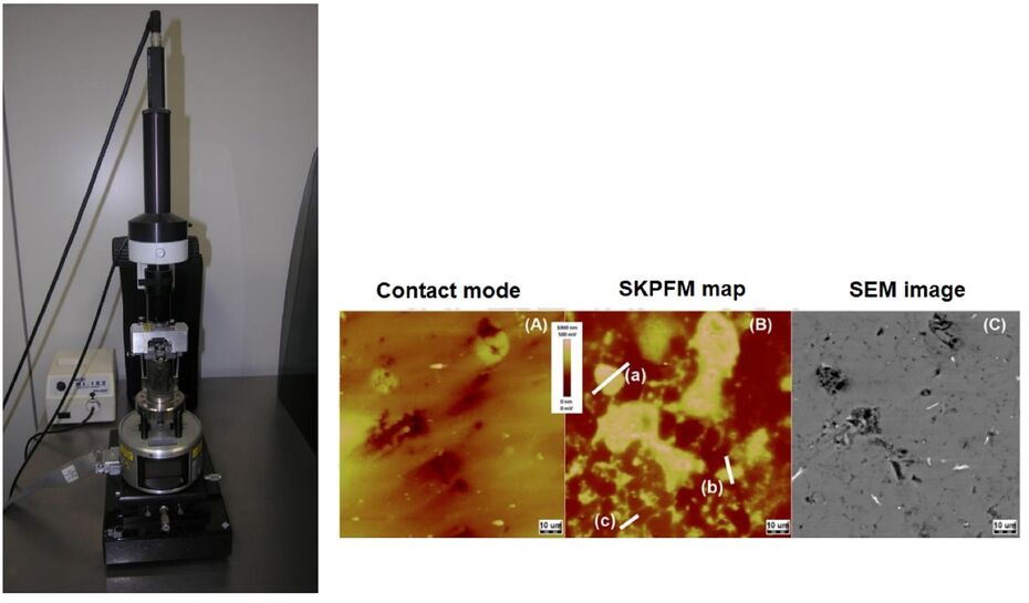
Atomic Force Microscope
The atomic force microscopy (AFM) is a technique for the investigation of the surface properties of different material with high spatial resolution. The AFM is typically employed for the acquisition of topographic maps with resolution in the nanometer range. This can be used to obtain information about the surface roughness of different materials including metals, polymers, ceramics and composites. Besides, the instrument available in our laboratory is equipped with the scanning Kelvin probe force microscopy technique (SKPFM) for the investigation of the surface potential (Volta potential). This technique, in particular in the case of metallic substrates, can be employed for the investigation of different phases and microstructure features. The SKPFM can be employed for the characterization of different metals and alloys including steel, aluminium, magnesium, copper and titanium alloys. This provides useful information for the interpretation of the corrosion behaviour at localized level and more in general, on the overall reactivity of metal surfaces.